Overview
Important
This documentation is under active construction. It’s intended to be the source of truth for all contributors and future maintainers. Reach out to socet@purdue.edu with questions!
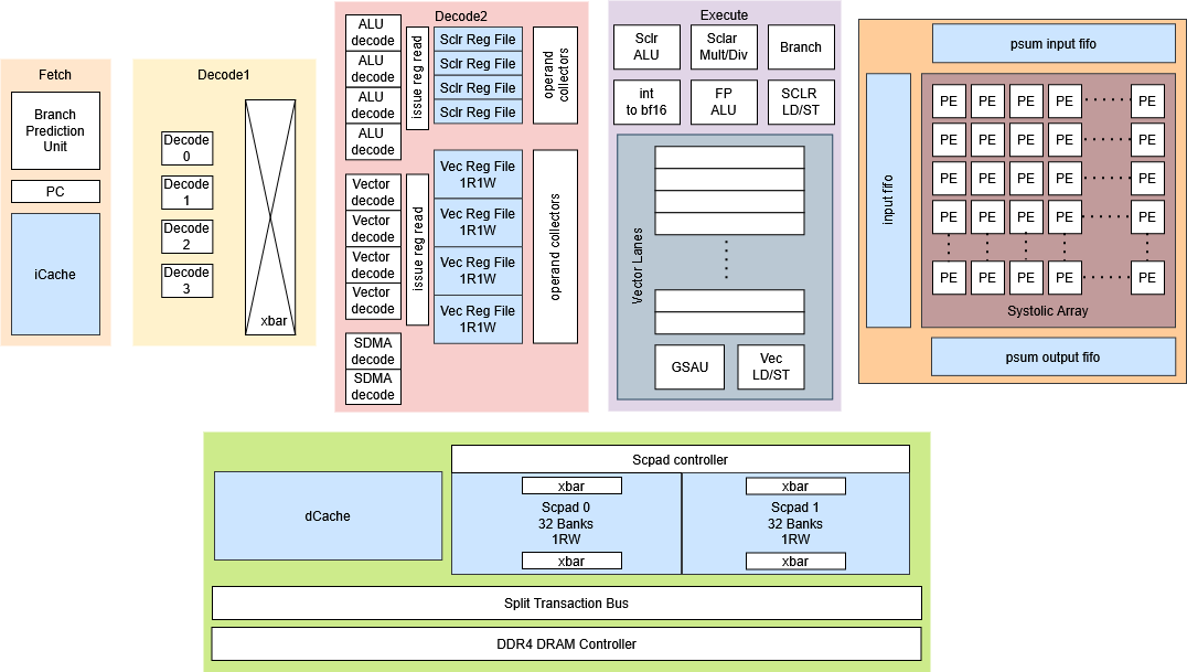
Atalla is a student-led effort within SoCET at Purdue University to design a research-grade AI accelerator stack end-to-end.
Modern deep-learning workloads demand high TOPS/W and predictable dataflow. Atalla explores a programmable accelerator architecture that is contributed to by the following teams:
- Compute: Systolic Array — parameterizable array with three implementations: naïve baseline, MEISSA-inspired, and TPU-inspired dataflows.
- On-Chip Memory: Scratchpad + Lockup-Free Caches — software-managed scratchpad hierarchy and non-blocking cache subsystem to keep compute saturated with predictable access.
- Memory System: DDR4 + Split-Transaction AXI4 — a non-blocking DDR4 controller and split-transaction interconnect; integrating Ramulator2-style timing models for flexible, cycle-accurate memory behavior.
- Systems Software: Kernels + PyTorch Flow — kernel implementations targeting the custom ISA, plus integration into a PyTorch-front-end workflow; includes emulator + cycle-accurate simulation.
- Compiler Toolchain (PPCI-based) — compiler infrastructure to lower high-level ops into the ISA and schedule memory movement.
- Hardware Scheduler: VLIW Control — VLIW-style scheduling hardware for deterministic, explicitly scheduled execution.
- Emulation: HAPS FPGA Bring-Up — deploy and validate the design on HAPS FPGA for hardware-in-the-loop testing.
This project aims to be an open, reproducible infrastructure that ties together the whole toolchain – from workloads to silicon-quality analysis: model-level experiments → architectural simulation → RTL design & verification → ASIC PPA flows → FPGA/emulation when available.
Note
Keywords: Computer Architecture · HW/SW Co-Design · Digital Verification · ASIC Synthesis · RTL Emulation
Guidelines / How-To
Setup Guidelines
This document should list any and all required steps to get yourselves setup to run Atalla. Specific setup scripts (like for the PyTorch infrastructure, or PPCI infrastructure) will be defined in sub-team homepages.
SSH into asicfab
The preferred IDE by the AI-HW team is VSCode. Please follow the instructions in DigitalOcean’s tutorial on connecting to a remote server.
You will need to download Cisco AnyConnect VPN if you plan to SSH from an out-of-campus location.
Setup asicfab
- Run
source /package/asicfab/AccountSetup/init.bash - Add the following into
~/.bashrc
[[ $- == *i* ]] || return
HOSTNAME=$(hostname)

if [ ${HOSTNAME} == "asicfab.ecn.purdue.edu" ]; then
        source /package/asicfab/AccountSetup/init.bash

        alias ls="ls --color"
        alias ll="ls -la"


        export COPYBUFFER=/package/asicfab/CopyBuffer
        export MODULEPATH=/package/asicfab/AccountSetup/modulefiles:$MODULEPATH
        export PATH=$HOME/.local/bin:$PATH # for python packages
        unset PYTHONPATH
        # For fusesoc + Questa usage
        export MODEL_TECH="$(dirname $(which vsim))"

        ###### CUSTOM CHANGES BELOW THIS LINE #######
        module load gcc/11.2.0 python3/3.11
        module load riscv-gcc verilator/5.036 gtkwave
        module load cadence/xcelium/23.03 siemens/questa/2021.4 intel/quartus-std
        module load lcov
elif [ ${HOSTNAME} == "asicfabu.ecn.purdue.edu" ]; then
        module load verilator gtkwave surfer lcov
else
        echo "Unknown host ${HOSTNAME}; not loading modules"
fi

module load cadence/genus       # used for synthesis
module load cadence/innovus     # used for physical implementation
module load cadence/virtuoso    # used for manually inspecting and manipulating the design
module load cadence/ssv         # good general module
module load cadence/ddi         # good general module

export LD_PRELOAD=/lib64/libz.so.1
Setup Github SSH
Follow the steps in the Github SSH-ing document. You should be able to clone the Atalla repository locally using git clone git@github.com:Purdue-SoCET/atalla.git now.
To test out a basic file, run
git checkout scratchpad_main
make run FILE=./scripts/common/xbar/clos/test.tcl
Synthesis
Overview
If you cloned the repository properly, and ran the setup scripts, you should be able to see “Flowkit” as a submodule. This is a repository compiled by the Design Flow team with a bunch of scripts/flows to help us use Genus and Innovus. It was initially a Cadence software, but it’s adapted.
Goals
You will use the following steps to compile each of your modules to get area and clock information. After this, look at the Reports step on how to format and store the reports that are generated.
Steps
The following steps outline what to do. Search for
@AIHWtag in each of the respective files to know where to add/edit stuff.
- Ensure you are in the
atallax01branch.
git checkout atallax01
git submodule update --init --recursive
- CREATE - /designs/cache/filelist.tcl
set listofdirs {}
lappend listofdirs "/home/asicfab/a/araviki/tensor-core/src/include"
set_db init_hdl_search_path $listofdirs

read_hdl -sv -define {NOIP SYNTHESIS} /home/asicfab/a/araviki/tensor-core/src/modules/cache_bank.sv
read_hdl -sv -define {NOIP SYNTHESIS} /home/asicfab/a/araviki/tensor-core/src/modules/cache_mshr_buffer.sv
read_hdl -sv -define {NOIP SYNTHESIS} /home/asicfab/a/araviki/tensor-core/src/modules/lockup_free_cache.sv
- EDIT - /scripts/config/design_config.tcl: search for “# Read Verilog and elaborate.”, and add this below
create_flow_step -name read_cache_hdl -owner design {
  source ./designs/cache/filelist.tcl
}

create_flow_step -name elaborate_cache -owner design {
  elaborate lockup_free_cache # replace with the name of your actual module
}
- EDIT - scripts/flow.yaml search for “flow: synthesis:”, near line 129
  synthesis:
    args: -tool genus -owner cadence -skip_metric -tool_options -disable_user_startup
    features:
    steps:
      - syn_generic:
          args: -owner cadence
          features:
          steps:
            - block_start:
            - init_elaborate:
            - init_design:
                args: -owner cadence
                features:
                steps:
                  - read_mmmc:
                  - read_physical:
                  # ########################
                  - read_cache_hdl: # replace this
                  - elaborate_cache: # replace this
                  # ########################
                  - read_power_intent:
                  - run_init_design:
                  - read_def:
                      enabled: "synth_ispatial || synth_hybrid"
- CREATE - /scripts/constraints/cache_bank.sdc. Always have interfaces for your modules. If you say it doesn’t need an interface, then that unit isn’t worth synthesizing alone.
set sdc_version 2.0

set_units -capacitance 1.0fF
set_units -time 1.0ps

# Set the current design
current_design cache_bank

# -period sets time in ps, 1000 -> 1GHz, 5000 -> 200Mhz
# -waveform = {-period}/2
create_clock -name "clock1" -period 1000.0 -waveform {0.0 500.0} [get_ports <interface_instance_name>_clk]

set_clock_transition -rise 1 [get_clocks "clock1"]
set_clock_transition -fall 1 [get_clocks "clock1"]
set_clock_uncertainty 0.1 [get_clocks "clock1"]

set_clock_gating_check -setup 0.0

set_driving_cell -lib_cell inv_8x -pin X [ all_inputs ] -min -max
set_input_delay -add_delay 1.0 -clock [get_clocks clock1] [all_inputs -no_clocks] # simulate 1ps delay
set_output_delay -add_delay 1.0 -clock [get_clocks clock1] [all_outputs]
- EDIT - scripts/setup.yaml search for “constraint_modes” near line 101
constraint_modes:
  func:
    sdc_files:
      - scripts/constraints/cache_bank.sdc
- RUN
Run the following commands in the Flowkit/ folder.
# Takes a long time
flowtool -reset -to synthesis

# Wakes up flowtool. It'll take a bit for all the required files to compile. You can run specific flow steps after this.
flowtool -flow run_syn_opt -interactive_run -isolate step
report_timing -max_paths 10 -path_type full > critical_paths.txt
Reports
Check within Flowkit/reports. reports/syn_opt/ has the results from the optimal synthesized flow. reports/syn_opt/qor.prt has the important content.
Create a folder for each submodule within tensor-core/reports, and store the relevant information in there. We will not gitignore it.
- To get the clock speed, take the {-period} value you set in /scripts/constraint/*.sdc file, and add the slack value. If clock period is (1000) and total slack is (-555) then the clock speed = (1/1555ps)MHz. If clock period is (3000) and total slack is (0) and Critical Path Slack is (1580.8), then your frequency is (1/(3000ps – 1580.8ps)) = 704.8MHz.
- To get the area, look under the Area section. Values are in (um)^2. 1(mm^2) = 1e-6(um)^2.
PCACTI
Ramulator2
Verification
Overview
Verification happens in three steps:
- Smoke Tests for all modules in SystemVerilog w/ QuestaSim.
- Unit Tests for individual modules in SystemVerilog w/ QuestaSim. Ensure you apply assertions and performance counters! The goal
- Top Level C++ tests w/ Verilator. This must be a more complete testbench, simulating real-workload situations.
All your code must go in ./tb/.
- ./tb/formal must contain all the mathematical assertions w/ covergroups.
- ./tb/unit must contain all the unit tests in the same heirarchy. Use
make sv_test folder= tb_file= GUI=to run QuestaSim. Check the Makefile for options. - ./tb/uvm is a maybe for now.
SoCET AI Hardware SystemVerilog Coding Guide
Written by: Malcolm McClymont
Last updated: 1/15/2026
Introduction
This guide is designed for engineers developing and testing hardware within the AI Hardware team. It provides a set of guidelines meant to facilitate large scale collaboration by making RTL code easy to read, modify, and test. These rules are split into three categories based on severity:
-
SHALL/SHALL NOT rules; these must be followed at (almost) all times. Any SHALL RULE VIOLATIONS must include comments that thoroughly explain how the rule is being violated and why. Anyone who deviates from these rules should not be surprised if asked to rewrite their code.
-
SHOUD/SHOULD NOT rules; these practices are strongly encouraged, but not strictly mandatory. Violating these rules does not require an explicit comment but may warrant rewriting code.
-
MAY/MAY NOT rules; these are practices that could improve code legibility or testability but are situational and should be applied at the engineer’s discretion.
Perceptive readers will notice that there are no absolute rules in this guide; engineers should always evaluate if a rule should be followed and provide documentation if they decide not to follow it.
Formatting
-
Engineers SHALL use spaces as tabs, with 4 spaces per tab.
VSCode can be configured to do this, but here are some commands for a .vimrc file that enables this:
autocmd BufNewFile,BufRead *.sv,*.v set tabstop=4 autocmd BufNewFile,BufRead *.sv,*.v set shiftwidth=4 autocmd BufNewFile,BufRead *.sv,*.v set expandtab -
Engineers SHALL minimize dead (commented out) code. If large sections of code are commented out (3 or more lines) then a pointer comment SHALL be used or the comment should be deleted.
-
Engineers SHALL consolidate code. Dead code and active code should be in separate groups, not intermixed.
An example of these two rules:
Bad! Notice how the dead and alive lines are mixed.

...

always_comb begin : input_buses
    // cu.input_type = 1'b0;
    cu.input_row = '0;
    cu.input_load = 1'b0;
    // cu.weight_row = '0;
    // cu.weight_load = 1'b0;
    cu.partials_row = '0;
    cu.partials_load = 1'b0;
    if (cu.input_en) begin
        cu.input_row = cu.row_in_en;
        cu.input_load = 1'b1;
    end else if (cu.weight_en) begin
        // cu.input_type = 1'b1;
        // cu.weight_row = cu.row_in_en;
        // cu.weight_load = 1'b1;
    end
    if (cu.partial_en) begin
        cu.partials_row = cu.row_ps_en;
        cu.partials_load = 1'b1;
    end
end

...
Better, dead lines are grouped together ... always_comb begin : input_buses cu.input_row = '0; cu.input_load = 1'b0; cu.partials_row = '0; cu.partials_load = 1'b0; // cu.weight_row = '0; // cu.weight_load = 1'b0; // cu.input_type = 1'b0; if (cu.input_en) begin cu.input_row = cu.row_in_en; cu.input_load = 1'b1; end else if (cu.weight_en) begin // cu.input_type = 1'b1; // cu.weight_row = cu.row_in_en; // cu.weight_load = 1'b1; end if (cu.partial_en) begin cu.partials_row = cu.row_ps_en; cu.partials_load = 1'b1; end end ...Best, pointer comments are used to move commented blocks away from the active code. Ideally, dead lines should be at end of file or deleted entirely. ... always_comb begin : input_buses cu.input_row = '0; cu.input_load = 1'b0; cu.partials_row = '0; cu.partials_load = 1'b0; //[1] if (cu.input_en) begin cu.input_row = cu.row_in_en; cu.input_load = 1'b1; end else if (cu.weight_en) begin //[2] end if (cu.partial_en) begin cu.partials_row = cu.row_ps_en; cu.partials_load = 1'b1; end end ... endmodule //[1] // cu.weight_row = '0; // cu.weight_load = 1'b0; // cu.input_type = 1'b0; //[2] // cu.input_type = 1'b1; // cu.weight_row = cu.row_in_en; // cu.weight_load = 1'b1; -
Signal names SHALL NOT exceed 30 characters. Additionally, their names SHOULD be intuitive.
-
Module names SHALL be intuitive.
-
All always_comb and always_ff blocks SHALL have names.
-
Blocks that share many signals or interact closely SHOULD be adjacent in the code. In other words, achieve spatial locality.
- However, always_comb blocks SHOULD be grouped with other always_comb blocks. The same applies to always_ff blocks.
-
Unless a block’s name makes its function obvious, every block SHOULD come with a comment describing what it does
For example:
//Detailed comment describing function of block always_comb begin : <block name> ... end ... //Detailed comment describing function of block always_ff begin : <block name> ... end -
Any outstanding fixes/modifications to code SHOULD be documented using a TODO comment
-
When applicable, RTL and code SHALL use “manager” and “subordinate” as opposed to “master” and “slave”.
Verilator Linter
-
Engineers SHALL NOT have any Verilator linter warnings in code within main branch
-
Engineers SHALL NOT use lint_off to disable warnings
- All of the Verilator warnings and their meanings can be found here: https://verilator.org/guide/latest/warnings.html
For example:
always_comb begin : <block name>
    ...

    //Bad! Why are they getting a truncate warning?
    //Engineer should explain this with a comment or fix it.

    /* verilator lint_off WIDTHTRUNC */
    curr_input_row = iteration[l];
    /* verilator lint_off WIDTHTRUNC */

    ...
end
Testbenches
- Engineers SHALL only print messages for failing test cases, but include a “test complete” message too. These failing tests SHALL include a timestamp.
For example:
//This will set %t to print in nanoseconds. Replace -9 with -12 for ps.
$timeformat(-9, 2, " ns");

...

if(tb_out != golden_out) begin
    $display("Output mismatch for test %0d at %0t", i, $time);
    failed_cases += 1;
end

...
-
Testbenches SHALL use `timescale 1ps/1ps.
-
TODO: Expand this section
Interfaces
- Engineers SHALL include an ifndef to avoid repeatedly including an interface
- Modports SHALL follow the format x_y, where x and y represent the two modules the interface connects
For example:
//Good

module backend #(parameter logic [SCPAD_ID_WIDTH-1:0] IDX = '0) (
    scpad_if.backend_sched bshif, //Connects backend to scheduler
    scpad_if.backend_body bbif,  //Connects backend to scratchpad body
    scpad_if.backend_dram bdrif //Conects backend to DRAM
);

...

endmodule
- TODO: Expand this section
Synthesizable Logic
- Plus and minus SHALL be the only arithmetic operators directly used in synthesizable logic.
For example:
//Good
assign c = a + b;
//Bad!
assign c = a * b;

//Good. Create an instance of an operational unit from a written Verilog module.
mult_module M0(.a(a), .b(b), .c(c))
-
When using a for loop in synthesizable code, its intended function SHALL be thoroughly commented. This also applies to generate for loops.
-
Any use of always_latch SHALL come with extensive documentation on its intended function.
-
Functions MAY be used in synthesized logic, but SHALL only contain combinational logic.
- SystemVerilog doesn’t actually support sequential logic in functions.
For example:
//Good, only contains combinational logic.
function [7:0] addition (input [7:0] in_a, input [7:0] in_b);
    addition = in_a + in_b;
endfunction

...

always_comb begin
    c = addition(a, b);
end
Combinational Logic
- Engineers SHALL NOT use nested ternary logic. Use an if/else or case block instead for this.
For example:
    //Bad! Nested ternary logic, hard to read.
    result = a ? b : c ? d : e;

    //Good. Use a different control structure.
    if(a) begin
        result = b;
    else if (c) begin
        result = d;
    else begin
        result = e;
    end

    //Also acceptable
    if(a) begin
        result = b;
    else begin
        result = c ? d : e;
    end
- Any modules that are fully combinational MAY have the clk and n_rst input signals removed.
Sequential Logic
-
Sequential elements SHALL only use posedge clk and negedge n_rst in their sensitivity lists.
-
Engineers SHALL only use packed arrays in synthesziable modules. Testbenches may use either packed or unpacked arrays.
For example:
logic [7:0] data; //Packed array
logic data [7:0]; //Unpacked array
-
FSMs SHALL always use enums as state names.
-
Engineers SHOULD always use explicit next_state logic.
-
Any sequential elements that do not strictly require an n_rst signal SHOULD NOT have one. However, you SHALL comment which elements do not have an n_rst signal
- Determining which elements do not need an n_rst signal SHOULD be done after the design is fully verified.
- Signals used for write enable by any modules SHALL always have an n_rst signal
Forbidden Structures
The following SystemVerilog structures SHALL NOT be used:
- Programs
- Fork/join
- Always@
- Z-state logic/tri-state buffers
- Classes and polymorphism SHALL be avoided. Typedef statements within packages SHALL be used instead.
- Any datatypes indicating the strength of a signal (supply1, strong1, weak1, etc.)
- Force statements
- Triple equal signs equality operators (===)
Direct Programming Interface‑C (DPI‑C)
Overview
The SystemVerilog Direct Programming Interface (DPI) provides a standard way to call C functions from SystemVerilog and to call SystemVerilog functions from C. The DPI forms a bridge between the two languages and allows re‑use of existing C/C++ models or libraries.
This guide walks through two complementary flows that combine DPI‑C and a parameterizable asynchronous FIFO. The first flow uses Verilator to convert a SystemVerilog FIFO into C++ and writes a C++ testbench. The second flow implements the FIFO in C++ and imports it into a SystemVerilog testbench via DPI‑C, targeting Siemens Questa SIM.
Sources
- SV DPI Tutorial
- Async FIFO RTL
- Running Verilator
- How to call C-functions from SV using DPI-C
- How to call SV-modules from C++ using DPI-C
Flow 1 – Verilating the SystemVerilog FIFO and Creating a C++ Testbench
a. Convert SystemVerilog to C++ with Verilator
Copy over async_fifo.sv into your local directory.
- Invoke Verilator:
verilator --cc async_fifo.sv --exe fifo_tb.cpp -CFLAGS "-std=c++17" --build
- –cc tells Verilator to generate C++ output.
- –exe fifo_tb.cpp requests Verilator to compile the provided C++ testbench and link it with the generated model.
- –build invokes make to build the executable.
- Run the compiled simulation:
./obj_dir/Vasync_fifo
Verilator will generate a directory (default obj_dir) containing C++ files for the design. The included fifo_tb.cpp drives the async_fifo model by toggling independent write and read clocks, writing a sequence of values, and reading them back. The testbench checks for ordering errors and prints “FIFO test passed” when successful. See the file fifo_tb.cpp for details.
b. Writing a C++ Testbench
The C++ testbench uses the Verilated model interface. After including Vasync_fifo.h and initializing reset signals, it toggles wclk and rclk at different rates to emulate independent clock domains. It drives w_en and r_en, monitors the w_full/r_empty flags and verifies correct FIFO operation.
Refer to fifo_tb.cpp.
Verilator’s generated wrapper class provides the public signals as C++ members. Remember to call top->eval() after changing inputs; this schedules and evaluates the model for the current timestep.
Flow 2 – Importing a C++ FIFO into a SystemVerilog Testbench via DPI‑C
a. Implement the FIFO in C++ and Expose it via DPI
Implementing a FIFO in C++ gives flexibility and allows using existing algorithmic models as golden references. The DPI‑C interface maps SystemVerilog types to C types; for example, byte maps to char and int maps to int. More complex types (arrays, 4‑state logic) require DPI‑defined types in svdpi.h. Arguments can be passed by value or reference depending on the argument direction.
The provided file dpi_fifo.cpp implements a simple power‑of‑two FIFO in C++. It defines a DpiFifo structure with depth, write and read pointers and a dynamically allocated array. The exported functions have extern “C” linkage so the names are not mangled. Key functions are defined in the dpi_hdr.h.
// Allocate a FIFO with at least the requested depth (rounded up to a power of two)
DpiFifo* fifo_init(int depth);
// Free the FIFO
void fifo_free(DpiFifo* fifo);
// Return non‑zero if FIFO is full
int fifo_full(const DpiFifo* fifo);
// Return non‑zero if FIFO is empty
int fifo_empty(const DpiFifo* fifo);
// Push/pop an integer; return 1 on success, 0 on full/empty
int fifo_push(DpiFifo* fifo, int data);
int fifo_pop(DpiFifo* fifo, int* data);
b. Import the C++ Functions into SystemVerilog
In the SystemVerilog testbench (sv_tb_dpi.sv) we declare the C functions using import “DPI-C”. The chandle type represents an opaque C pointer. The testbench allocates the FIFO, pushes a sequence of integers, pops them back and checks the order:
module tb;
    import "DPI-C" function chandle fifo_init(input int depth);
    import "DPI-C" function void    fifo_free(input chandle handle);
    import "DPI-C" function int     fifo_push(input chandle handle, input int data);
    import "DPI-C" function int     fifo_pop(input chandle handle, output int data);
    import "DPI-C" function int     fifo_full(input chandle handle);
    import "DPI-C" function int     fifo_empty(input chandle handle);
    // … allocate and use FIFO …
endmodule
c. Compile and Run with Questa SIM
Siemens’ Questa SIM automatically compiles and links DPI‑C code when using the vlog -dpiheader option. The Elektroda article summarises the steps:
Write your C function and compile it into a position‑independent shared object (.so on Linux).
Declare the function in SystemVerilog using import “DPI-C” ….
Compile both C and SystemVerilog files together with vlog, then run the simulation and load the shared object with vsim -sv_lib.
vlib work
vlog -dpiheader dpi_hdr.h dpi_fifo.cpp sv_tb_dpi.sv
vsim -c work.tb -do "run -all; quit"
The -dpiheader switch instructs vlog to generate a header (dpi_hdr.h) that contains the prototypes of the imported functions. Questa automatically calls GCC to compile the C file and link the resulting shared library. Alternatively you can pre‑compile the C library manually:
gcc -fPIC -shared -I$MTI_HOME/include -o libdpi.so dpi_fifo.cpp
vlog sv_tb_dpi.sv
vsim work.tb -sv_lib libdpi
Be sure that the C library is compiled for the same word size as your simulator (32‑bit vs. 64‑bit); otherwise you will see linker errors. Also remember to include svdpi.h in your C file; without it the DPI data types are undefined.
Appendix
FIFO RTL
Adapted from https://www.verilogpro.com/asynchronous-fifo-design/.
// async_fifo.sv
module async_fifo #(
    parameter int DATA_WIDTH = 8,
    parameter int ADDR_WIDTH = 4
) (
    input  logic               wclk,
    input  logic               wrst_n,
    input  logic               w_en,
    input  logic [DATA_WIDTH-1:0] wdata,
    output logic               w_full,
    input  logic               rclk,
    input  logic               rrst_n,
    input  logic               r_en,
    output logic [DATA_WIDTH-1:0] rdata,
    output logic               r_empty
);
    localparam int FIFO_DEPTH = 1 << ADDR_WIDTH;
    logic [DATA_WIDTH-1:0] mem [0:FIFO_DEPTH-1];
    logic [ADDR_WIDTH:0] wptr_bin, rptr_bin;
    logic [ADDR_WIDTH:0] wptr_gray, rptr_gray;
    logic [ADDR_WIDTH:0] wptr_gray_sync1, wptr_gray_sync2;
    logic [ADDR_WIDTH:0] rptr_gray_sync1, rptr_gray_sync2;

    // Write domain
    always_ff @(posedge wclk or negedge wrst_n) begin
        if (!wrst_n) begin
            wptr_bin  <= '0;
            wptr_gray <= '0;
        end else if (w_en && !w_full) begin
            mem[wptr_bin[ADDR_WIDTH-1:0]] <= wdata;
            wptr_bin  <= wptr_bin + 1;
            wptr_gray <= (wptr_bin + 1) >> 1 ^ (wptr_bin + 1); // binary→Gray
        end
    end

    // Read domain
    always_ff @(posedge rclk or negedge rrst_n) begin
        if (!rrst_n) begin
            rptr_bin  <= '0;
            rptr_gray <= '0;
        end else if (r_en && !r_empty) begin
            rptr_bin  <= rptr_bin + 1;
            rptr_gray <= (rptr_bin + 1) >> 1 ^ (rptr_bin + 1);
        end
    end

    // Data output; asynchronous read with registered output
    always_ff @(posedge rclk) begin
        rdata <= mem[rptr_bin[ADDR_WIDTH-1:0]];
    end

    // Synchronize Gray pointers across domains
    always_ff @(posedge wclk or negedge wrst_n) begin
        if (!wrst_n) begin
            rptr_gray_sync1 <= '0;
            rptr_gray_sync2 <= '0;
        end else begin
            rptr_gray_sync1 <= rptr_gray;
            rptr_gray_sync2 <= rptr_gray_sync1;
        end
    end
    always_ff @(posedge rclk or negedge rrst_n) begin
        if (!rrst_n) begin
            wptr_gray_sync1 <= '0;
            wptr_gray_sync2 <= '0;
        end else begin
            wptr_gray_sync1 <= wptr_gray;
            wptr_gray_sync2 <= wptr_gray_sync1;
        end
    end

    // Full and empty detection:contentReference[oaicite:8]{index=8}
    always_comb begin
        // Empty when synchronized write pointer equals local read pointer
        r_empty = (wptr_gray_sync2 == rptr_gray);
        // Full when MSBs differ and lower bits match
        w_full  = (wptr_gray[ADDR_WIDTH] != rptr_gray_sync2[ADDR_WIDTH]) &&
                  (wptr_gray[ADDR_WIDTH-1:0] == rptr_gray_sync2[ADDR_WIDTH-1:0]);
    end
endmodule
FIFO TB in C++
// fifo_tb.cpp
// -----------------------------------------------------------------------------
// C++ testbench for async_fifo.sv when Verilated into C++.
//
// Build idea (typical):
// verilator -Wall --cc async_fifo.sv --exe fifo_tb.cpp --top-module async_fifo
// make -C obj_dir -f Vasync_fifo.mk
// ./obj_dir/Vasync_fifo
//
// Verilator's guide describes translating SV to C++ with --cc and building an
// executable with --binary/--exe.citeturn583946675001164
// -----------------------------------------------------------------------------
#include <cstdint>
#include <deque>
#include <iostream>
#include <random>
#include "Vasync_fifo.h"
#include "verilated.h"
static vluint64_t main_time = 0;
static void tick(Vasync_fifo* top) {
top->eval();
main_time++;
}
int main(int argc, char** argv) {
Verilated::commandArgs(argc, argv);
auto* top = new Vasync_fifo;
// Simple async clocks: write clock toggles every cycle, read clock every 2
top->wclk = 0;
top->rclk = 0;
top->wrst_n = 0;
top->rrst_n = 0;
top->w_en = 0;
top->r_en = 0;
top->w_data = 0;
// apply reset
for (int i = 0; i < 10; i++) {
top->wclk = !top->wclk;
if ((i % 2) == 0) top->rclk = !top->rclk;
tick(top);
}
top->wrst_n = 1;
top->rrst_n = 1;
std::deque<uint32_t> scoreboard;
std::mt19937 rng(1);
std::uniform_int_distribution<int> coin(0, 1);
const int N = 2000;
for (int t = 0; t < N; t++) {
// drive enables in their own domains
bool do_write = (coin(rng) == 1);
bool do_read = (coin(rng) == 1);
// Write domain on rising edge of wclk
if (!top->wclk) {
top->w_en = do_write;
if (do_write) {
uint32_t v = (uint32_t)t;
top->w_data = v;
}
}
// Read domain on rising edge of rclk
if (!top->rclk) {
top->r_en = do_read;
}
// toggle clocks
top->wclk = !top->wclk;
if ((t % 2) == 0) top->rclk = !top->rclk;
tick(top);
// Scoreboard updates after edges
if (top->w_en && !top->w_full) {
scoreboard.push_back(top->w_data);
}
if (top->r_en && !top->r_empty) {
if (scoreboard.empty()) {
std::cerr << "ERROR: DUT popped but scoreboard empty\n";
return 2;
}
uint32_t exp = scoreboard.front();
uint32_t got = top->r_data;
scoreboard.pop_front();
if (got != exp) {
std::cerr << "ERROR: mismatch exp=" << exp << " got=" << got << "\n";
return 3;
}
}
}
std::cout << "PASS\n";
delete top;
return 0;
}
FIFO C++
// dpi_fifo.cpp
// -----------------------------------------------------------------------------
// C++ async FIFO model exposed through a C ABI for SystemVerilog DPI-C.
//
// This is the "C++ golden model -> SV testbench" flow.
// - SV holds a handle (chandle) to an allocated C++ object.
// - SV calls fifo_push/fifo_pop each cycle or transaction.
//
// DPI-C uses svdpi.h types and API; keeping types consistent matters because
// SV<->C data must be interpreted identically.citeturn818598791849910
// -----------------------------------------------------------------------------
#include <cstdint>
#include <cstdlib>
#include <new>
#include <vector>
extern "C" {
#include "svdpi.h"
}
struct FifoU32 {
explicit FifoU32(int depth_pow2)
: depth(depth_pow2), mem((size_t)depth_pow2, 0) {
reset();
}
void reset() {
wptr = 0;
rptr = 0;
}
bool empty() const { return wptr == rptr; }
bool full() const {
int mask = depth - 1;
return ((wptr & mask) == (rptr & mask)) && (((wptr ^ rptr) & depth) != 0);
}
bool push(uint32_t v) {
if (full()) return false;
mem[(size_t)(wptr & (depth - 1))] = v;
wptr = (wptr + 1) & ((2 * depth) - 1);
return true;
}
bool pop(uint32_t* out) {
if (empty()) return false;
*out = mem[(size_t)(rptr & (depth - 1))];
rptr = (rptr + 1) & ((2 * depth) - 1);
return true;
}
int depth;
std::vector<uint32_t> mem;
int wptr{0};
int rptr{0};
};
extern "C" {
// Create a FIFO. depth must be power-of-2.
void* fifo_create(int depth) {
try {
return new FifoU32(depth);
} catch (...) {
return nullptr;
}
}
void fifo_destroy(void* h) {
delete static_cast<FifoU32*>(h);
}
void fifo_reset(void* h) {
if (!h) return;
static_cast<FifoU32*>(h)->reset();
}
// Returns 1 on success, 0 on full
int fifo_push_u32(void* h, unsigned int v) {
if (!h) return 0;
return static_cast<FifoU32*>(h)->push((uint32_t)v) ? 1 : 0;
}
// Returns 1 on success, 0 on empty
int fifo_pop_u32(void* h, unsigned int* out_v) {
if (!h || !out_v) return 0;
uint32_t tmp = 0;
if (!static_cast<FifoU32*>(h)->pop(&tmp)) return 0;
*out_v = (unsigned int)tmp;
return 1;
}
int fifo_empty(void* h) {
if (!h) return 1;
return static_cast<FifoU32*>(h)->empty() ? 1 : 0;
}
int fifo_full(void* h) {
if (!h) return 0;
return static_cast<FifoU32*>(h)->full() ? 1 : 0;
}
} // extern "C"
FIFO C++ Header
// cpp_async_fifo.h
// -----------------------------------------------------------------------------
// Simple parameterizable FIFO model in C++ (power-of-2 depth)
// Used as a pure C++ golden model *or* inside DPI wrappers.
// -----------------------------------------------------------------------------
#pragma once

#include <array>
#include <cstddef>
#include <cstdint>

// Depth must be power-of-2.
template <typename T, std::size_t DEPTH>
class AsyncFifo {
    static_assert((DEPTH & (DEPTH - 1)) == 0, "DEPTH must be power-of-2");

public:
    AsyncFifo() { reset(); }

    void reset() {
        wptr_ = 0;
        rptr_ = 0;
    }

    bool empty() const { return wptr_ == rptr_; }

    bool full() const {
        // full when lower bits match but MSB differs
        const std::size_t mask = DEPTH - 1;
        return ((wptr_ & mask) == (rptr_ & mask)) && ((wptr_ ^ rptr_) & DEPTH);
    }

    bool push(const T& v) {
        if (full()) return false;
        mem_[wptr_ & (DEPTH - 1)] = v;
        wptr_ = (wptr_ + 1) & ((DEPTH * 2) - 1);
        return true;
    }

    bool pop(T& out) {
        if (empty()) return false;
        out = mem_[rptr_ & (DEPTH - 1)];
        rptr_ = (rptr_ + 1) & ((DEPTH * 2) - 1);
        return true;
    }

private:
    std::array<T, DEPTH> mem_{};
    // pointers carry one extra wrap bit -> range [0, 2*DEPTH)
    std::size_t wptr_{0};
    std::size_t rptr_{0};
};
FIFO TB in SV
// sv_tb_dpi.sv
// -----------------------------------------------------------------------------
// SystemVerilog testbench that imports a C++ FIFO model via DPI-C.
//
// Questa compile notes (one common flow):
// - Compile SV + C together with vlog and autolink
// - Or compile C into a shared library and load with vsim -sv_lib
// Example commands appear in many guides; one common pattern is:
// vlog -dpiheader dpi_hdr.h dpi_func.c tb_top.sv
// vsim -c work.tb_top -do "run -all; quit"citeturn115040724918351
// -----------------------------------------------------------------------------
module tb_dpi_fifo;
import "DPI-C" function chandle fifo_create(input int depth);
import "DPI-C" function void fifo_destroy(input chandle h);
import "DPI-C" function void fifo_reset(input chandle h);
import "DPI-C" function int fifo_push_u32(input chandle h, input int unsigned v);
import "DPI-C" function int fifo_pop_u32 (input chandle h, output int unsigned v);
import "DPI-C" function int fifo_empty(input chandle h);
import "DPI-C" function int fifo_full (input chandle h);
chandle h;
int unsigned got;
localparam int DEPTH = 16;
initial begin
h = fifo_create(DEPTH);
if (h == null) $fatal(1, "fifo_create failed");
fifo_reset(h);
// push 0..DEPTH-1
for (int i = 0; i < DEPTH; i++) begin
if (!fifo_push_u32(h, i)) $fatal(1, "unexpected full at i=%0d", i);
end
if (!fifo_full(h)) $display("NOTE: fifo_full() did not assert; check full policy");
// pop and check
for (int i = 0; i < DEPTH; i++) begin
if (!fifo_pop_u32(h, got)) $fatal(1, "unexpected empty at i=%0d", i);
if (got !== i[31:0]) $fatal(1, "mismatch exp=%0d got=%0d", i, got);
end
if (!fifo_empty(h)) $display("NOTE: fifo_empty() did not assert; check empty policy");
fifo_destroy(h);
$display("PASS");
$finish;
end
endmodule
Introduction to the Atallax01 Programming Model
The Atallax01 Programming Model allows users to map C/C++ algorithms to throughput-focused deep-learning accelerator, architected around VLIW vector-datapath, SW-managed Scratchpad and a 32x32 BF16 Systolic Array.
Unlike GPUs, Atallax01 does not expose a wide SIMT/SIMD programming interface. Instead, it provides a tile-centric compute model where kernels explicitly optimize and orchestrate data movement, vector lane utilization and Systolic Array computations through a single unified instruction stream. The workloads that will be run on Atalla are highly regular and need both wide-and-deep pipelines specifically for two-dimensional matrices.
Atallax01 is not a general-purpose processor. It is a core that will be placed alongside a high-performance CPU for a heterogenous compute plateform. Programmability is offered through C/C++ and a custom compiler toolchain. We do not plan to support imperative languages like Python.
This document defines:
- the hardware execution model
- the memory heirarchy
- the programming constructs available to the user
- tile-based psuedocode conventions
Hardware Differences
CPUs are computing machines that were fine-tuned over decades to minimize the latency of single-threaded instruction streams. They rely heavily on advanced techniques like prediction, speculaton, dynamic scheduling, etc. SMT, a computing perspective that partitioned/allocated register-sets to time-mulitplex independent software threads, was added as an afterthought into a single CPU core to exploit even more instruction-level parallelism.
However, the industry saw the need for different machines to exploit the data-level parallelism seen in scientific and graphics workloads. GPUs are massively-parallel computing machines, primarily programmed using CUDA or HIP paradigms which expose implicit-SIMD perspectives to the user. This enables the user to write scalar-threaded code in C++ which are compiled into SIMT binaries to utilize the SIMD execution units. CUDA inintially innovated by combining hardware-efficiency of SIMD but the programmability of SMT.
In recent years, GPUs been adapted to cater to the demand of the deep learning ecosystem with the addition of Tensor Cores for matrix-multiplications. TPUs grew parallely, but were targeted purely for deep-learning workloads that were domainted by GEMMs/CONVs. Atallax01 targets these primitives directly and disregards the SIMT/SIMD abstractions. Users will write single-thread code in C/C++ that directly defines tile-based descriptors for memory movement and vector-based kernels for compute datapaths. Thus, we say Atallax01 behaves more like a TPU than a GPU.
Heterogenous Programming
Atallax01 is programmed using a heterogenous host-device model, similar in spirit to CUDA/HIP but fundamentally simpler.
Host responsibilities include: - Allocate DRAM Tenstors. - Launch device kernels. - Pass tile descriptors and kernel metadata. Device responsibilities include: - Move data between DRAM and on-chip SRAM. - Swizzle data within the Scratchpad to enable row/coloumn-major addressing. - Load slices of the tiles into vector registers. - Execute blocking vector load/store/compute operations to prime the Systolic Array, or utilize the execution lanes.
The compiler issues VLIW bundles into a mapped-space within the DRAM partition exposed to Atallax01. The on-chip scheduling unit enforces a tainted-VLIW scheme by checking dependencies through scoreboarding.
Memory Model
The Atallax01 memory system is software-managed, and does not enforce any hardware-managed ordering mechanisms. The datapath is in-order, with the SDMA instructions making SCPAD locations valid before later accesses take place.
Global Memory (DRAM): - Large, high latency - Only accessible via SDMA instructions. - Ideal for storing large tensors. Assume 8GB+ space. Scratchpad Memory (SCPAD): - 1MB SRAM on-chip memory, low latency. - Only accessible via SDMA instructions. - Two seperate partitions indexed as SCPAD0 and SCPAD1 Vector Register File (VEGGIE): - [X-Size] SRAM vector-register-file - Only accessible via VM instructions. - Intermediate tile-slice storage to send to Lanes/Systolic-Array Scalar Register File: - [X-Size] SRAM lockup-free D-Cache - Implemented as a hardware-managed L1 Cache. Systolic Array Accumulation Buffers: - Not programmable. Hardware-controlled. - Strided/Staggered collection and tranfer of vectors into VEGGIE.
Execution Model
VLIW-based execution. Each cycle, the scheduler may one of [X] Packet types. The compiler ensures intra-bundle independence, with inter-bundle dependencies handled by the Scoreboardds in the Scheduler Unit.
In the following sections, we will focus on explaining the different “concepts” to keep in mind before developing code for Atallax01. Following this, we will discuss abstracted kernels which utilize these concepts.
Abstract Entities:
TileDesc       - 2D block of memory Global/Scpad (described by shape + strides)


GlobalRegion   - Where in Global Memory
GlobalTile     – N-D tensor in off-chip DRAM, has-a Global Region

ScpadRegion    - Which Scratchpad and where inside the Scratchpad
ScpadTile      – 2D tensor in on-chip SRAM, has-a TileDesc and ScpadRegion

VectorReg[v]   – vector register(s) in the vector core
Abstract Instrinsics:
SDMA_LD_* ScpadTile, GlobalTile
SDMA_ST_* ScpadTile, GlobalTile
VM_LD VectorReg[v], ScpadTile
VM_ST VectorReg[v], ScpadTile
VV_* VectorReg[v], VectorReg[v]
VV_* VectorReg[v], Imm
VS_* VectorReg[v], ScalarReg[v]

GEMMV ScpadTile C, ScpadTile A, ScpadTile B
CONV ScpadTile C, ScpadTile A, ScpadTile B
Kernels
General Matrix-Multiply (GEMM)
Atallax01 does not expose 32x32 Systolic Array directly. Instead, we provide a fixed-shape sub-kernels that operate on tiles that satisfy [<= 32x32].
Let’s define
TM  – rows of the output tile   (TM ≤ 32)
TN  – cols of the output tile   (TN ≤ 32)
TK  – reduction dimension slice (TK ≤ 32)
A single GEMMV instrinsic consumes:
A_tile  : TM × TK  (activations)
B_tile  : TK × TN  (weights)
C_tile  : TM × TN  (partial sums / output)
and computes:
C_tile = A_tile · B_tile + C_tile
entirely inside the vector-core + systolic array microcode, blocking until SPCAD_C is updated.
Tiling/Grouping
Given a standard GEMM of general dimensions
C[M × N] = A[M × K] · B[K × N]
we can decompose it into the following number of tiles:
MT = ceil(M / TM)
NT = ceil(N / TN)
KT = ceil(K / TK)
Each output tile C[i,j] (for 0 ≤ i < MT, 0 ≤ j < NT) is defined as:
C_tile(i,j) = C[ i*TM : (i+1)*TM,   j*TN : (j+1)*TN ]
A_tile(i,k) = A[ i*TM : (i+1)*TM,   k*TK : (k+1)*TK ]
B_tile(k,j) = B[ k*TK : (k+1)*TK,   j*TN : (j+1)*TN ]
All three of these tiles are loaded into on-chip SRAM as ScpadTiles before a GEMMV call.
Below, we define the tiling logic:
struct TileGroupDesc {
    GlobalTile A_g;   // TM x TK slice of A in DRAM
    GlobalTile B_g;   // TK x TN slice of B in DRAM
    GlobalTile C_g;   // TM x TN slice of C in DRAM
    int i, j, k;      // tile indices (row, col, k reduction)
}

vector<TileGroupDesc> plan_gemmv(
    GlobalTile A, GlobalTile B, GlobalTile C,
    int M, int N, int K,
    int TM, int TN, int TK
) {
    vector<TileGroupDesc> groups;

    for (int i = 0; i < M; i += TM) {
      for (int j = 0; j < N; j += TN) {

        GlobalTile C_g = make_tile(C, i, j, TM, TN);

        for (int k = 0; k < K; k += TK) {

          GlobalTile A_g = make_tile(A, i, k, TM, TK);
          GlobalTile B_g = make_tile(B, k, j, TK, TN);

          groups.push_back(TileGroupDesc{.A_g = A_g, .B_g = B_g, .C_g = C_g, .i = i, j = j, .k = k});
        }
      }
    }

    return groups;
}
Execution Loop
Note: _alloc_scpad0, _alloc_scpad1 and _gemmv are functions defined in the stub library we provide with the E2E stack. It works at the vector-register level.
bool execute_gemmv(
    GlobalTile A, GlobalTile B, GlobalTile C,
    int M, int N, int K
) {
    const int TM = ...; // ≤ 32
    const int TN = ...; // ≤ 32
    const int TK = ...; // ≤ 32

    vector<TileGroupDesc> groups = plan_gemmv(A, B, C, M, N, K, TM, TN, TK);

    for each distinct (i, j) over output tiles {
        GlobalTile C_g = pop_group(i,j, groups).C_g;

        ScpadTile sc_C  = _alloc_scpad1(TM, TN);
        SDMA_LD_1(sc_C, C_g);

        for each g in groups where (g.i == i and g.j == j) {
            in order of g.k {

                // Using different register spaces within the Scratchpad allows the compiler
                // to packetize to allow overlapping loads while compute happens.
                ScpadTile sc_A  = _alloc_scpad0(TM, TK);
                ScpadTile sc_B  = _alloc_scpad1(TK, TN);
                SDMA_LD_0(sc_A, g.A_g);
                SDMA_LD_1(sc_B, g.B_g);

                _gemmv(sc_C, sc_A, sc_B);
            }
        }

        SDMA_ST_1(sc_C, C_g);
    }
}
HW Architecture
Caches
Lockup-Free D/I Cache
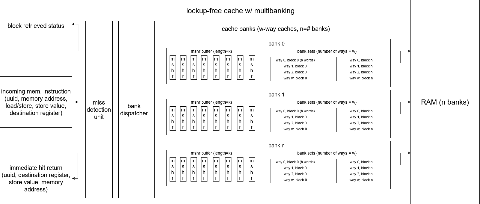
This project implements a lockup-free, multi-banked cache intended for integration with the SoCET AIHW and GPU cores. The design allows cache hits to complete independently of outstanding misses, while supporting multiple in-flight memory requests via per-bank MSHR queues.
The cache is fully parameterized (capacity, associativity, block size, banks, MSHR depth) and written in synthesizable SystemVerilog. The implementation targets realistic OoO scheduling behavior rather than simplified blocking semantics.
Architectural Overview
At the top level, the cache is organized as N independent banks, each containing:
- a set-associative cache array
- a per-bank MSHR buffer
- replacement logic
- a bank-local control FSM
Incoming memory operations are classified in a multi-cycle FSM as:
- hit → serviced immediately by the target bank
- miss → enqueued into that bank’s MSHR buffer
Critically, hits and misses are serviced in parallel. In a single cycle, the design supports:
- up to N concurrent misses (one per bank)
- one hit resolution concurrently
Miss completion is decoupled from request issue via UUID tagging, allowing the processor to continue execution without stalling on outstanding memory operations.
Banking and Set Interleaving
Banks partition the total set space rather than duplicating full cache structures. Set indices are interleaved across banks to maximize spatial parallelism:
bank_id = global_set_index % NUM_BANKSbank_set_index = global_set_index / NUM_BANKS
This mapping allows sequential memory accesses (e.g., streaming through arrays) to naturally distribute across banks, enabling parallel block fills and reducing structural hazards. Banking also shortens tag-compare critical paths and aligns with multi-bank DRAM interfaces where available.
Miss Status Holding Registers (MSHRs)
Each bank contains a FIFO-style MSHR buffer that tracks outstanding misses. An MSHR entry represents one cache block, not individual words.
Each MSHR stores:
- block address
- valid bit
- per-word write mask
- buffered store data (for store misses)
- UUID associated with the originating instruction
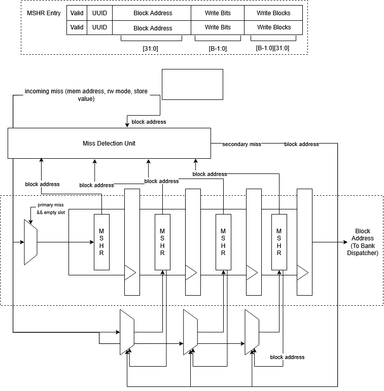
Secondary Miss Coalescing
If a miss arrives for a block already present in the buffer, it is coalesced into the existing MSHR:
- store misses update the word mask and buffered data
- load misses reuse the same pending fill
This significantly reduces redundant memory traffic for spatially clustered accesses, a common pattern in OoO execution.
The buffer is implemented as a shift-based pipeline rather than pointer-indexed queue:
- new entries enter at the tail
- entries advance toward the head when unstalled
- the head MSHR is latched into the bank for processing
Latency added by shifting is negligible relative to DRAM service time.
Bank Operation and Hit-Under-Miss
Each bank exposes two independent access paths:
- Direct hit path for new memory instructions
- MSHR head path for servicing outstanding misses
On a hit:
- tag comparison across all ways
- load returns data in the same cycle
- store updates data and dirty bit
On a miss:
- victim way selected
- victim invalidated before refill to prevent hit-after-evict hazards
- block fill applied
- buffered store data merged
- UUID returned upon completion
MSHR Hit Resolution
A key corner case arises when a secondary miss reaches the bank after the primary miss has already been latched. To handle this, the bank performs MSHR hit detection:
- detects that the requested block is already resident (or in flight)
- suppresses unnecessary refetch
- allows pending writes to be applied correctly
This preserves correctness without forcing full reserialization of misses.
Replacement Policy
Replacement uses an age-based LRU implementation:
- each way maintains an age counter
- on access, selected way resets to age 0
- all others increment
- max-age way is precomputed as victim
This approach generalizes cleanly to arbitrary associativity but introduces a long combinational path, which became the dominant timing bottleneck in synthesis.
Currently, tree-based (pseudo-LRU) is being added to reduce comparator depth and critical path length.
Verification and Results
The design was fully unit-tested and system-tested. Verified behaviors include:
- hit-under-miss
- secondary miss coalescing
- MSHR corner cases
- replacement correctness
- basic load/store ordering
Synthesis (MIT-LL 90nm PDK) achieved:
- ~643 MHz post-synthesis frequency
- dominant critical path in LRU and MSHR comparison logic
The architecture is functionally complete but intentionally left open for pipeline refinement and timing-driven simplification.
DRAM Subsystem Homepage
Introduction
The DRAM subsystem exists to provide the Atalla accelerator with access to off-chip memory required by AI workloads that exceed on-chip SRAM limits. Because DRAM access involves strict command sequencing and long latencies, a controller and memory bus are required to manage these accesses. This subsystem’s current goals are towards a non-blocking architecture that improves bandwidth by overlapping memory requests.
This page serves as the central home for the DRAM Subsystem. It consolidates RTL diagrams, active projects, reports, presentations, and ramp-up material. Use the links below to navigate based on what you are looking for.
-
New to the DRAM subsystem?
Follow the ramp-up guide for background, architecture context, and recommended resources -> Ramp-Up Guide
-
Working on the DRAM subsystem?
View active projects, current contributors, development branches, and documentation -> Active Projects
-
View Past Reports/Presentations?
View past reports, presentations, abstracts, and posters made by the DRAM subsystem -> Past Reports and Presentations
-
View completed projects?
View completed projects by the DRAM subsystem -> Completed Projects
Ramp-Up Guide
This section is for new students joining the DRAM subsystem and serves as a starting point for getting up to speed. It includes background material and resources to help you understand the design and begin contributing.
-
Introductory DRAM Overview (Recommended Starting Point)
A high-level video explaining the basic structure and operation of DRAM. This is an excellent first exposure and helps build intuition before diving into more technical material.
https://www.youtube.com/watch?v=7J7X7aZvMXQ&t=47s
-
Memory Systems: Cache, DRAM, Disk – Jacob, Ng, and Wang
Chapters 10-13 are required reading as they provide depth on DRAM organization, timing, and memory system.
https://purdue.primo.exlibrisgroup.com/discovery/fulldisplay?docid=alma99169138574101081
-
Understanding DDR4 Timing Parameters
A short reference page summarizing DDR4 timing parameters and constraints.
https://www.systemverilog.io/design/understanding-ddr4-timing-parameters/
-
JEDEC DDR4 Standard (JESD79-4C)
The official DDR4 specification defining all command sequences, timing requirements, and constraints
https://raw.githubusercontent.com/RAMGuide/TheRamGuide-WIP-/main/DDR4%20Spec%20JESD79-4C.pdf
-
ETH Zurich Lecture: DRAM Controllers (Prof. Onur Mutlu)
An in-depth lecture covering DRAM controller design, performance challenges, and architectural tradeoffs.
https://www.youtube.com/watch?v=TeG773OgiMQ
Active Projects
This section documents the currently active DRAM subsystem projects, including their purpose, implementation status, code locations, and points of contact.
Non-Blocking DRAM Controller
Description: The goal of this project is to design a non-blocking DRAM controller that allows multiple memory requests to be in flight simultaneously to improve bandwidth utilization. The design uses a row-open policy and bank-specific request queues to hide memory latency and enable memory-level parallelism.
Contributors
- Jason Lyst (jlyst@purdue.edu)
- Adrian Buczkowski (abuczko@purdue.edu)
- Eddie Hu (hu927@purdue.edu)
- Shams Hoque (hoques@purdue.edu)
RTL Diagrams
This sections links the location of all Block-/RTL-diagrams that were made for this design: https://app.diagrams.net/#G18bqekF9I8oZJpSTm-BcsDvPkOPy_cdul#%7B%22pageId%22%3A%22fpKTT8HEuwSpTkvlEaWT%22%7D
Active Branches
This section links the location of active branches that are being used for the design:
- Main DRAM Branch: https://github.com/Purdue-SoCET/atalla/tree/ddr_cntrl
Architecture Overview The design of Non-blocking Memory Controller was based around using queues and arbiters to maximize the throughput of data. Memory requests flow in from the split-transaction AXI, which then connect to the Read ID and Load Queue (Load Requests), as well as the Write Data and Store Queue (Store Requests). These requests are processed through a frontend arbiter, which balances the ratio of request types, and the backend arbiter, which uses a Command FSM to determine the timing of bank/bank group activation and readiness. This then allows for multiple requests to occur in flight.
Key Files
└── rtl/
    ├── include/
    │   └── ddr_cntrl/
    │       ├── dram_pkg.svh           # Package definitions (timings, commands)
    │       └── ddr_controller_if.sv   # Top-level interface for the controller
    ├── modules/
    │   ├── common/
    │   │   └── general/
    │   │       └── fifo.sv            # Generic FIFO utility
    │   └── ddr_cntrl/
    │       ├── ddr_controller_wrapper.sv # Top-level module integration
    │       ├── frontend_arb_nb.sv     # AXI front-end arbitration logic
    │       ├── address_mapper.sv      # AXI address to DRAM Rank/Bank/Row/Col
    │       ├── nb_store_queue.sv      # Store queue for non-blocking writes
    │       ├── load_queue_nb.sv       # Load queue for non-blocking reads
    │       ├── nb_bank_queue.sv       # Bank-specific transaction tracking
    │       ├── cmd_fsm_nb.sv          # Main Command FSM for DDR protocols
    │       ├── fsm_module.sv          # Sub-FSM logic components
    │       ├── nb_barb.sv             # Bank Arbiter for Command Generator
    │       ├── refresh_counter.sv     # Periodic refresh management
    │       ├── nb_wdata_wrapper.sv    # Write data path integration
    │       ├── nb_wdata_queue.sv      # Buffering for write data
    │       ├── nb_read_id_queue.sv    # Tracking AXI IDs for out-of-order reads
    │       ├── flex_counter.sv        # Parametric counter utility (With rollover)
    │       ├── flex_sr.sv             # Parametric shift register
    │       ├── priority_enc.sv        # Priority encoder for arbiters
    │       └── enum_compare.sv        # Comparison logic for FSM states
└── tb/
  └── unit/
      └── ddr_cntrl/
          └── testbench/
              ├── dram_top_tb.sv            # Top - this connects to Micron TB
              ├── frontend_tb.sv            # Frontend
              ├── init_state_tb.sv          # State Machine tb
              ├── nb_barb_tb.sv             # Backend Arbiter
              ├── nb_wdata_queue_tb.sv      # Write Path Queue
              └── refresh_counter_tb.sv     # Simulation
Usage
Within the scripts folder(scripts/ddr_cntrl), there are TCL scripts to run the various modules as well as the top level. Using them only requires that the same Makefile that is found in the branch to be used, specifically the section that reads
## Example:
## 		make run FILE=./scripts/xbar/benes_rom/verify.tcl
## 		make run FILE=./scripts/memory/scratchpad/swizzle/verify.tcl
run:
  vsim -do "source $(FILE)"
run_sim:
  vsim -c -do "source $(FILE)"
- Use the scripts as a base to iterate, with -c to test for command line only (i.e. debugging compilation/elaboration errors)
- This model uses the Micron TB found within the protected_modelsim folder, so it is necessary for the folder to be in the branch during operation - WARNING: THE TOP LEVEL CAN ONLY BE RAN WITH A SPECIFIC BASHRC WRITTEN BELOW
  # Check that shell is interactive
  [[ $- == *i* ]] || return
  HOSTNAME=$(hostname)

  if [ ${HOSTNAME} == "asicfab.ecn.purdue.edu" ]; then
    source /package/asicfab/AccountSetup/init.bash

    alias ls="ls --color"
    alias ll="ls -la"


    export COPYBUFFER=/package/asicfab/CopyBuffer
    export MODULEPATH=/package/asicfab/AccountSetup/modulefiles:$MODULEPATH
    export PATH=$HOME/.local/bin:$PATH # for python packages
    unset PYTHONPATH
    # For fusesoc + Questa usage
    export MODEL_TECH="$(dirname $(which vsim))"

    ###### CUSTOM CHANGES BELOW THIS LINE #######
    module load git/2.18.0 gcc/11.2.0 python3/3.11
    module load riscv-gcc verilator/5.028 gtkwave
    module load cadence/xcelium/23.03 siemens/questa/2021.4 intel/quartus-std
    module load lcov
  elif [ ${HOSTNAME} == "asicfabu.ecn.purdue.edu" ]; then
    module load verilator gtkwave surfer lcov
  else
    echo "Unknown host ${HOSTNAME}; not loading modules"
  fi


  # Set prompt
  source $HOME/.bash/git-prompt.sh
  export GIT_PS1_SHOWDIRTYSTATE=true
  export GIT_PS1_SHOWSTASHSTATE=true
  export GIT_PS1_SHOWCOLORHINTS=true
  export PROMPT_COMMAND='__git_ps1 "\[\e]0;\u@\h: \w\a\]\[\033[01;32m\]\u@\h\[\033[00m\]:\[\033[01;34m\]\w\[\033[00m\]" "\$ "'
- The assumption is made that the regular asicfab setup as already been completed for this to work. Note - while the bashrc may look similar, no work has been done to truly determine why top doesn’t work with the regular bashrc. Future work can be done to check why before iterating on this design.
Design Documentation/Resources
This section links any documentation or resources that was used specific for this design. This includes meeting notes, design logs, research papers, etc.
- https://ieeexplore.ieee.org/document/7108455
- https://cdn.discordapp.com/attachments/1412834335983272129/1421965427600392203/dram_controller_non_block_idea.pdf?ex=69792800&is=6977d680&hm=67a75be2ec3b113caa3017cc4007acdce61c7919d64f179cc3b22d7cfcef2005&
- DDR4 MICRON Model: https://drive.google.com/file/d/1CKYhZJe7rzhp_2ATkkAfWrufMl-Lt6jW/view?usp=sharing
Split-Transaction Interconnect
Description: The goal of this project is to design a split-transaction memory bus that can manage simultaneous in-flight requests from caches/scratchpad and simultaneous in-flight responses from the DRAM controller.
Contributors
- Aryan Kadakia (kadakia0@purdue.edu)
- Xinyu Liu (liu3680@purdue.edu)
RTL Diagrams
This sections links the location of all Block-/RTL-diagrams that were made for this design: https://app.diagrams.net/#G18bqekF9I8oZJpSTm-BcsDvPkOPy_cdul#%7B%22pageId%22%3A%22fpKTT8HEuwSpTkvlEaWT%22%7D
Active Branches
This section links the location of active branches that are being used for the design:
- Aryan Kadakia’s Branch: https://github.com/Purdue-SoCET/atalla/tree/memory_subsystem_aryan#
- Main DRAM Branch: https://github.com/Purdue-SoCET/atalla/tree/memory_subsystem_dram
Verification
This section links the location of verification related documents like verification plans:
Design Documentation/Resources
This section links any documentation or resources that was used specific for this design. This includes meeting notes, design logs, research papers, etc.
- https://developer.arm.com/documentation/102202/0300/AXI-protocol-overview
- https://www.cis.upenn.edu/~cis5710/spring2024/slides/13_axi.pdf
Ramulator Integration and Verification
Description
The Ramulator Integration project builds an AXI4-compliant wrapper around the Ramulator2 cycle-accurate DRAM simulator, allowing the full Atalla memory subsystem (caches, scratchpads, AXI bus) to be verified against realistic DRAM timing without designing a new memory controller for each DRAM standard. Swapping a YAML configuration file is all that is required to switch between DDR4, HBM3, or any other standard that Ramulator2 supports, making it the primary verification and design-space exploration vehicle for the DRAM team.
Why This Was Built
Every time the team wanted to test a different DRAM standard or configuration, a new RTL controller had to be designed and verified from scratch. This project eliminates that cost by wrapping Ramulator2 — which already models DDR4, HBM2, HBM3, LPDDR5, and others — behind a fixed AXI4 interface. The rest of the system never changes; only the YAML config changes. The wrapper is also intended to become the long-term DRAM interface for the Atalla TPU as the project matures.
Architecture Overview
The integration consists of two tightly coupled layers:
-
SV Wrapper (
rtl/modules/memory/ramulator_wrapper/ramulator_sv_wrapper.sv): An AXI4 subordinate that accepts AR/R/AW/W/B channel traffic from the memory bus. It manages a Re-Order Buffer (ROB) for burst reads, a serial FIFO for single-beat reads, and all flow-control backpressure signals. It communicates with Ramulator exclusively through DPI-C function calls. -
C DPI Bridge (
rtl/modules/memory/ramulator_wrapper/ramulator_dpi.cpp): Implements all DPI-C functions called by the SV wrapper. It instantiates Ramulator2, maintains a functional memory model for immediate write forwarding and partial-write merging, and coalesces burst read beats into single DRAM CAS commands to reduce row activations.
The DRAM standard and timing parameters are fully specified by a YAML configuration file passed at simulation start. No RTL changes are needed when switching standards.
Tools and Frameworks
| Tool | Purpose |
|---|---|
| Ramulator2 | Cycle-accurate DRAM simulator (C++); models DDR4, HBM2, HBM3, LPDDR5, and more |
| QuestaSim / ModelSim | SystemVerilog simulator; runs the SV wrapper and testbenches |
| DPI-C | IEEE standard mechanism for calling C/C++ functions from SystemVerilog |
| CMake + gcc-toolset-14 | Builds libramulator_dpi.so from ramulator_dpi.cpp and the Ramulator2 sources |
| Python 3 | Utility scripts: gen_sdma_meminit.py, sweep.sh result parser |
Environment Setup
These steps need to be done once per machine before running any simulation.
-
Run the setup script — appends
ATALLA_ROOTandUVM_HOMEto your~/.bashrc:make setup source ~/.bashrc -
Verify gcc-toolset-14 is accessible — the build requires GCC 14, installed at
/opt/rh/gcc-toolset-14/. No manualscl enableis needed; the Makefile invokes the compiler by absolute path automatically. -
Build the Ramulator DPI shared library — this compiles
ramulator_dpi.cppand all Ramulator2 sources intolibramulator_dpi.so:make ram_libThis step is required before any simulation target and is run automatically by
make simandmake sdma. Expect it to take several minutes on first build; subsequent builds are incremental. -
Generate the SDMA memory init file — needed only for the SDMA testbench; produces
configs/sdma_meminit.bin:make gen_sdma_meminit
Key Files
rtl/modules/memory/ramulator_wrapper/
├── ramulator_sv_wrapper.sv      # AXI4 SV wrapper
├── ramulator_dpi.cpp            # C DPI bridge to Ramulator2
├── ramulator_dpi.h              # DPI-C function declarations
├── gen_sdma_meminit.py          # Generates binary meminit for SDMA test
└── configs/
    ├── ddr4_config.yaml         # Default DDR4 config
    ├── hbm3_config.yaml         # Default HBM3 config
    ├── ddr4_1ch_128b.yaml       # DDR4 sweep variant: 1 channel, 128-bit bus
    ├── ddr4_1ch_256b.yaml       # DDR4 sweep variant: 1 channel, 256-bit bus
    ├── ddr4_2ch_128b.yaml       # DDR4 sweep variant: 2 channels, 128-bit bus
    ├── ddr4_1ch_512b.yaml       # DDR4 sweep variant: 1 channel, 512-bit bus
    ├── ddr4_4ch_128b.yaml       # DDR4 sweep variant: 4 channels, 128-bit bus
    ├── hbm3_1ch_2pc_32b.yaml    # HBM3: 1 physical channel, 2 pseudochannels
    ├── hbm3_8ch_2pc_32b.yaml    # HBM3: 8 physical channels, 2 pseudochannels
    ├── hbm3_16ch_2pc_32b.yaml   # HBM3: 16 physical channels, 2 pseudochannels
    └── sdma_meminit.bin         # Pre-built 1024×1024 int16 matrix binary

tb/unit/memory/ramulator_wrapper/
├── test_ramulator.sv            # Basic wrapper functional test
└── test_sdma.sv                 # SDMA matrix-load benchmark

scripts/
├── sweep.sh                     # Runs make sdma across all configs; saves logs to results/
└── parse_results.py             # Parses results/*.log and writes results/summary.csv
Running Examples
All targets build libramulator_dpi.so automatically if it is out of date.
Basic wrapper test (single config):
make sim                                    # DDR4, batch mode
make sim DRAM=hbm3                          # HBM3, batch mode
make sim CFG=rtl/modules/memory/ramulator_wrapper/configs/ddr4_1ch_256b.yaml
make sim GUI=ON                             # open QuestaSim waveform viewer
SDMA matrix-load benchmark (requires meminit):
make sdma SDMA_MEMINIT=rtl/modules/memory/ramulator_wrapper/configs/sdma_meminit.bin
make sdma SDMA_MEMINIT=... BURST=1          # burst read mode
make sdma SDMA_MEMINIT=... CFG=rtl/modules/memory/ramulator_wrapper/configs/hbm3_config.yaml
Configuration sweep across all DDR4 and HBM3 variants:
bash scripts/sweep.sh          # single-beat mode; logs saved to results/*_single.log
bash scripts/sweep.sh 1        # burst mode;       logs saved to results/*_burst.log
python3 scripts/parse_results.py results/   # parse logs, print summary table, write results/summary.csv
YAML Configuration
Each YAML file fully specifies the simulated DRAM. The key parameters are:
MemorySystem:
  DRAM:
    impl: DDR4          # or HBM3, HBM2, LPDDR5, ...
    org:
      preset: DDR4_8Gb
      channel: 1        # number of channels (HBM: counts pseudochannels)
      channel_width: 128  # bus width in bits per channel
    timing:
      preset: DDR4_2400R
To add a new configuration, copy an existing YAML from configs/, change impl, channel, channel_width, and timing, then pass it via CFG=<path>.
Contributors
- Heng-I (Ivor) Chu (chu244@purdue.edu) — SV wrapper, C DPI bridge, functional memory model, testbench, AXI transaction emulator
- Akram Mohamed (mahmoud6@purdue.edu) — HBM3 support, Ramulator interface
Active Branches
- Ivor’s Branch: https://github.com/Purdue-SoCET/atalla/tree/axi_ramulator_ivor
- Main Ramulator Branch: https://github.com/Purdue-SoCET/atalla/tree/axi_ramulator_main
Verification
test_ramulator.sv: Exercises read/write correctness and backpressure handling for the SV wrapper. Tests include read-after-write, raw reads, read/write backpressure, simultaneous read/write, multiple outstanding transactions, all three AXI burst types (INCR, FIXED, WRAP), and byte-strobe partial writes. All read data is checked against a shadow memory reference model.test_sdma.sv: Loads a 1024×1024 int16 matrix in both row-major (1024-element rows) and tile-major (32×32-element tiles) order. Reports total cycles, wall time at 800 MHz, cycles per matrix row, cycles per 8-beat transfer, cycles between beats, effective bandwidth in B/cycle, and AR stall percentage.
Benchmark Results Summary
The SDMA benchmark was run across 8 memory configurations at 800 MHz. Key findings:
- More channels beats wider interface: Going from 1→2→4 DDR4 channels at 128-bit width nearly doubles throughput each step, while widening the interface from 128b to 512b at 1 channel actually reduces throughput (wider bus without more parallelism increases stall).
- Burst mode helps most under bandwidth pressure: DDR4 1ch 128b jumps from ~11 B/cycle to ~30 B/cycle switching from single-beat to burst mode. High-bandwidth configs (DDR4 4ch, all HBM3) show little additional gain from burst mode since they are already near peak.
- HBM3 reaches ~32 B/cycle with 0% stall even at 1 channel, comparable to DDR4 4-channel, due to its pseudo-channel architecture and strong bank-level parallelism. Adding more HBM3 channels beyond 1 shows no further improvement on this workload, indicating the memory system is no longer the bottleneck.
- Tile-major access helps on bandwidth-limited DDR4 (better row locality reduces bank conflicts) but has negligible impact on high-bandwidth configs where the workload is already compute-bound.
Design Documentation/Resources
- https://github.com/CMU-SAFARI/ramulator2
Past Reports and Presentations
This section lists all past final reports, presentations, abstracts, and any other resource that was made by the DRAM subsystem.
Final Reports
- Fall 2025 Final Report: https://docs.google.com/document/d/1fIBgyiB3g3OImUYkugq2czNFDmUUhIS_DO6sGcxqxDY/edit?usp=sharing
- Spring 2025 Final Report: https://docs.google.com/document/d/1J7sHHt2H2yTATN91Cda57GuU_zQYz0v8/edit?usp=sharing&ouid=112766930685277737014&rtpof=true&sd=true
Design Review Presentations
- Fall 2025 Design Review 1: https://purdue0-my.sharepoint.com/:p:/g/personal/khatri12_purdue_edu/IQDGPSESbApgR6gN1-VNOP-jAaiWMO0WYFC02s4PZF21BJo?e=WBqsit
- Fall 2025 Design Review 2: https://purdue0-my.sharepoint.com/:p:/g/personal/khatri12_purdue_edu/IQBl4rWfHvqdT4ZHBKWouYAqAawxNiz32_OpBjLJoTGnRlo?e=8q3a8d
- Spring 2025 Design Review: https://purdue0-my.sharepoint.com/:p:/g/personal/khatri12_purdue_edu/IQCThlgQtvIaQbjwHBnV-sbAAddkki-xSmsUfsxGS6OnpZE?e=lCDwWu
Abstracts
- Fall 2025 Abstract: https://purdue0-my.sharepoint.com/:w:/g/personal/khatri12_purdue_edu/IQANqWleEbkvT5E5I8LGPdeWAcWw7mlhg-Q2tpLF6bX1JFc?e=gO85O0
Poster Presentation
- Fall 2025 Poster Presentation: https://purdue0-my.sharepoint.com/:p:/g/personal/khatri12_purdue_edu/IQC-xhWrYXVmSrW5sevR7zQ1AegyEuAUWBxusv5jGvgEdPo?e=OTz2Ys
Completed Projects
Blocking DRAM Controller
Description: The goal of this project is to design a fully functional DRAM Controller that interfaces with a ddr4 model.
Contributors
- Tri Than (than0@purdue.edu)
- Dhruv Khatri (khatri12@purdue.edu)
RTL Diagrams
This sections links the location of all Block-/RTL-diagrams that were made for this design: https://app.diagrams.net/#G18bqekF9I8oZJpSTm-BcsDvPkOPy_cdul#%7B%22pageId%22%3A%22fpKTT8HEuwSpTkvlEaWT%22%7D
Active Branches
This section links the location of active branches that are being used for the design:
- Tri’s Branch: https://github.com/Purdue-SoCET/atalla/tree/memory_subsystem_tri
- Dhruv’s Branch: https://github.com/Purdue-SoCET/atalla/tree/memory_subsystem_dhruv
- Main DRAM Branch: https://github.com/Purdue-SoCET/atalla/tree/memory_subsystem_dram
Verification
This section links the location of verification related documents like verification plans:
Design Documentation/Resources
This section links any documentation or resources that was used specific for this design. This includes meeting notes, design logs, research papers, etc.
- DDR4 MICRON Model: https://drive.google.com/file/d/1CKYhZJe7rzhp_2ATkkAfWrufMl-Lt6jW/view?usp=sharing
Scheduler
Scratchpad
Scratchpad V1
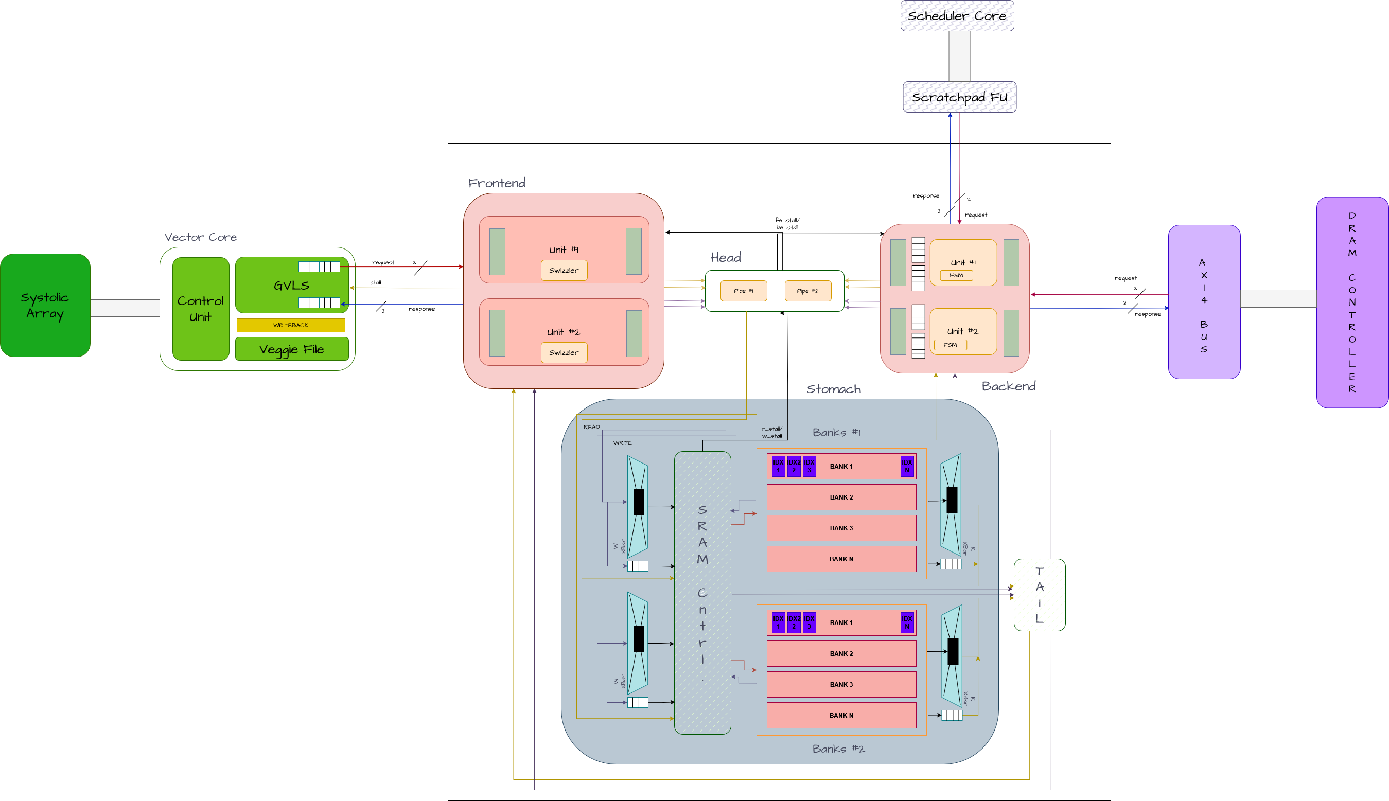
Modern AI Accelerators, like the Atalla Ax01 core, depend on exploiting predictable, high-bandwidth data movement between on-chip memory and compute modules. The Machine Learning (ML) workloads that these specialized chips target inherently expose deterministic access patterns – including tiled matrix multiplication, toeplitz-based convolution, tensor transposes and vector operations. The memory primitive in such architectures are arrays, often called vectors, as opposed to the scalar-optimized general-purpose chips. Additionally, these chips implement memory hierarchies that rely on conventional cache designs, accommodating a wide variety of workloads. These mechanisms are defined by tag overheads, unpredictable latencies, and hardware-based prefetchers that are optimized for adapting to different workload characteristics at runtime.
In order to study alternate designs that exploit the aforementioned data regularity, Atalla Ax01’s “Scratchpad” architecture implements a parameterizable software-controlled memory subsystem that combines (1) a tile-descriptor-based DMA engine (2) SRAM-banking strategies evaluated on different technology nodes, and (3) four multi-stage interconnect topologies that re-arrange vectors on-the-fly. The architecture provides for swizzle-based movement, avoiding bank-conflicts for wide vector-reads and transpose-friendly micro-op scheduling.
A core component of the explored design space were the interconnect micro-architectures - Benes, Batcher-Banyan, CLOS - simply referred to as crossbars. All designs were synthesized on the MIT-LL 90nm CMOS process node, and optimized for area, power and clock frequency. A Python-based emulator was built to confirm the viability of the design for the targeted behaviour, and simulated against every possible data-access pattern. The micro-architecture was implemented and modelled at a gate-level using SystemVerilog - within the industry-standard QuestaSim - achieving code coverage of 90%+.
The work accomplished by this team has laid the foundation for a hardware-software co-designed kernel library that will provide optimized implementations of core vector and matrix operations. In parallel, a custom compiler is being developed to lower this code into instruction bundles, enabling parallel execution of µ-ops to use the asynchronous data-movement features of the Scratchpad. The Atalla Ax01 accelerator will feature a 4-wide tainted-VLIW scheduler, split-transaction AXI-bus and dual-channel DDR4 controller to complement the Scratchpad design.
Systolic Array
Systolic Array Architectures
Weight-Stationary Systolic Array
Description:
Block Diagram: Top Level
Code:
Important Architecture Decisions:
Verification:
MEISSA
Description: The MEISSA (Multiplying Matrices Efficiently in a Scalable Systolic Architecture) design performs GEMM (General Matrix Multiplication). The design is parameterized to support FP16 and BF16 data types.
Block Diagram: 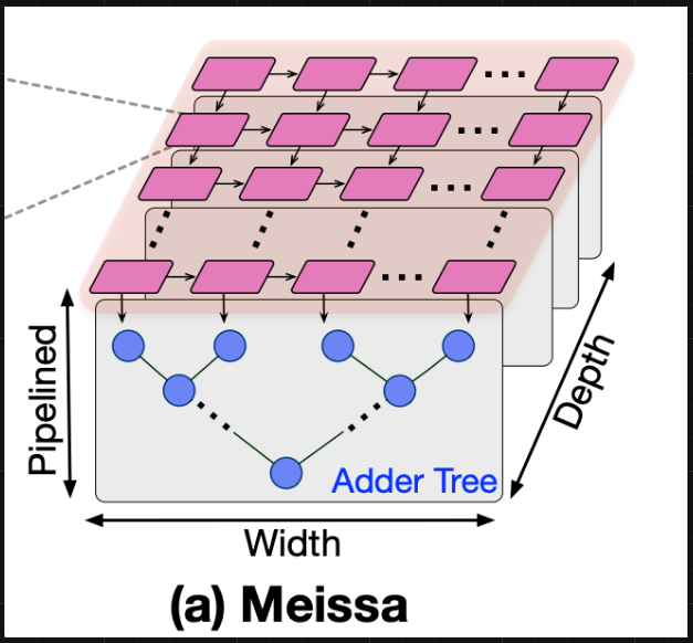
Code: here
Important Architecture Decisions: The architecture was based on this Georgia Tech paper. The MEISSA design decouples the MAC units into a multiplier grid and an adder tree for each column. This allows inputs to enter the multiplier grid without staggering, removing the need for an input buffer. MEISSA uses a weight stationary approach, where weights are input as columns then held in the multipliers. Activations are then sent in row-wise and stream through the multiplier grid and adders. MEISSA produces outputs along the diagonals of the result matrix. A wraparound output buffer is used to organize these outputs into rows.
Verification:
Reference Used: Georgia Tech Paper
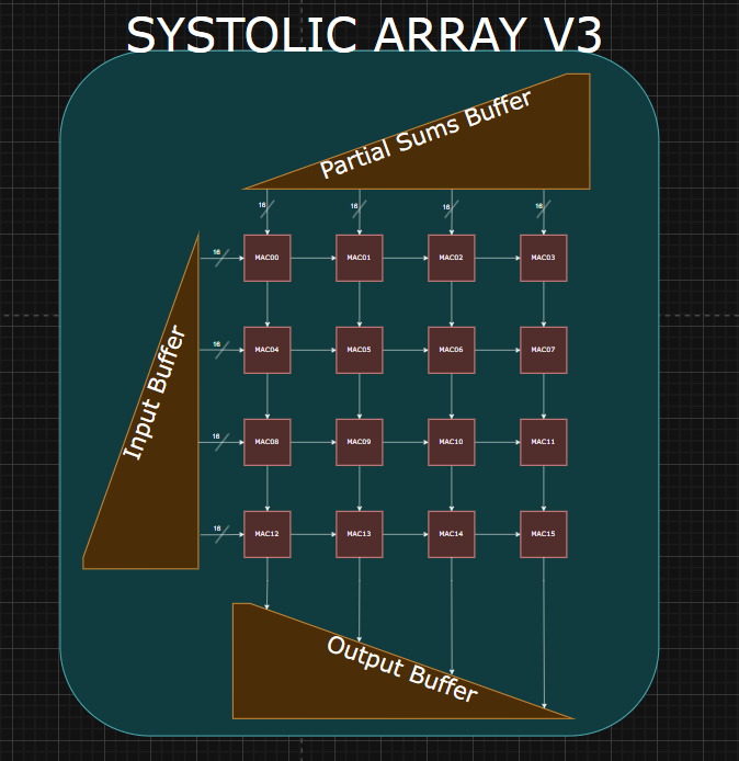
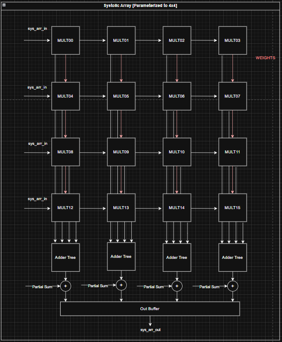
TPU Style
Description: The TPU (Tensor Processing Unit) design preforms GEMM. The implementation is parameterized to support FP16 and BF16 data types.
Block Diagram: 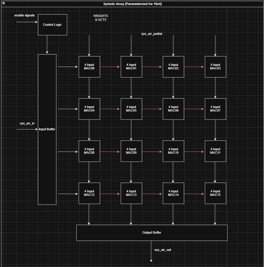
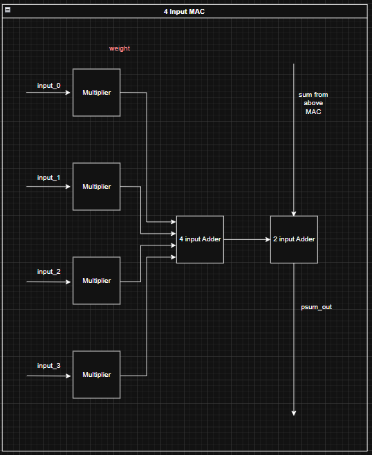
Code: here
Important Architecture Decisions: This architecture is based on this Google TPU Patent. The design uses a weight stationary approach where weights are loaded in columns-wise and held in the multiplier. The activation matrix is stored into an input buffer, and inputs to the multipliers are staggered in groups of 4. The outputs of the TPU are staggered so an output buffer is used to organize the result into rows.
Verification:
Reference Used: Google TPU Patent
Arithmetic Modules
4-Input Floating Point Adder
Description: The 4-input floating point adder performs fused addition of 4 floating point values. The HDL is parameterized to support various standard and non-standard floating point formats, including FP16, FP32, and BF16.
Block Diagram: 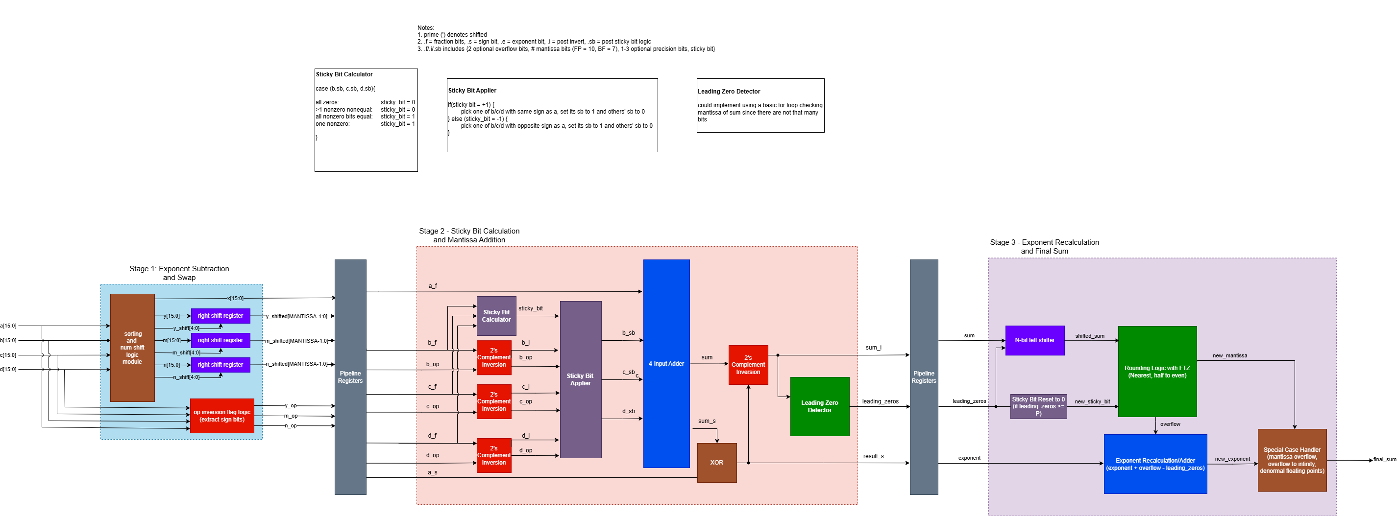
Code: https://github.com/Purdue-SoCET/atalla/blob/4_input_fp_adder/rtl/modules/systolic_array/sysarr_4_input_fp_adder.sv
The adder contains three pipelined stages
- Exponent Alignment and Mantissa Expansion
- Stage 1 Addition
- Stage 2 Addition, LZD, Exponent Recalculation, Mantissa Normalization, and Final Output
Important Architecture Decisions: The architecture was based on this IEEE paper (https://ieeexplore.ieee.org/document/11008646). The adder implements DAZ and FTZ logic for simplicity and speed.
The exponent alignment stage determines the largest of the four input exponents and calculates the difference between it and the other three exponents. The mantissa is expanded with 22 precision bits and shifted according to the exponent differences.
The second stage inverts the mantissas according to the sign bits of the original operands and performs a fused addition. The first stage of the addition uses a carry-save adder for speed.
The third stage uses a ripple carry adder to finish the addition operation, and uses a tree-based LZD to detect leading zeroes. The mantissa is rounded to the original format using rounding to nearest, half to even logic. The exponent is recalculated based on LZD and rounding overflow, and the final output is compiled, taking into account special cases detected in the exponent alignment stage.
Verification:
- The adder was verified through testing against the Berkeley Softfloat Library (https://github.com/ucb-bar/berkeley-softfloat-3).
- The testbenches can be found here: https://github.com/Purdue-SoCET/atalla/blob/4_input_fp_adder/tb/unit/systolic_array/.
- The test cases generation scripts can be found here: https://github.com/Purdue-SoCET/atalla/blob/4_input_fp_adder/scripts/systolic_array/.
Reference Used: https://ieeexplore.ieee.org/document/11008646
Vector-Core Documentation Homepage
Author: Vedant Sharma
Revision #: 0.1.0
Page Status: Under Active Development
Introduction
Hello, and welcome to the Vector-Core Documentation page of Atalla.
The Vector-Core is a custom datapath for the Atalla Accelerator created in order to take advantage of Data Level Parallelism (DLP). Vector-Core does this by performing compute upon vector-elements, effectively utilizing Single Instruction Multiple Data operations to increase performance. The design enables parallel execution of identical operations commonly used in AI workloads across multiple execution lanes.
This page serves as both a technical reference and centralized hub for the Architecture, RTL Diagrams, Verification Methodology, Synthesis Reports, Presentations, and Reports related to the Vector-Core Subsystem.
The goal of this page is to provide clear documentation of the work being done, onboarding material for new contributors, and detailed specifications for active development of Vector-Core.
-
New to Vector-Core?
Take a look at the onboarding guide for a bit of background, architectural overview, and primer material resources to help get started.
-
Working on Vector-Core?
View and/or update active projects, development branches, and documentation tied to Vector-Core.
-
View High-Level Architecture
View the current Vector-Core architecture.
-
View Past Documentation
View prior reports, presentations, and posters created by the Vector-Core team.
Onboarding Guide
This is for new students joining the Vector-Core in order to provide ample resources to catch up on the current state of Vector-Core and getting started. The material provided here is highly reccommended to review as it can aid in understanding of design choices and give you the knowledge to start contributing.
-
Medium - SIMD Primer Article (Recommended Starting Point)
An article covering starter concepts for SIMD Architecture, provides easy to follow visual examples. Gives a high-level explanation behind the basic premises of Vector-Core and why it’s necessary in Atalla. Would recommend reading this article before diving in-depth through the Fall 2025 Report and the Onur Mutlu Lecture.
https://medium.com/e4r/a-primer-to-simd-architecture-from-concept-to-code-d3cc470d6709 -
Vector-Core Fall 2025 Report
The Fall 2025 Vector-Core team’s Final Report, if you want to be a master of understanding the base of vector-core, this is the place to look. Although certain designs may have changed it will still provide value in learning design processes. Try to see if you can figure out optimizations on your own, or compare the prior designs to current designs, observe the flaws and how they were fixed.
https://docs.google.com/document/d/1cg5F1VhrnKALM-ZJHYC2e-JDQ-3BDk2Ngdvvg9fJhPw/edit?usp=sharing -
ETH Zürich Lecture: SIMD Architecture
A detailed lecture covering different SIMD architecures such as a Vector Processing Unit, the limitations & challenges that come with Vector-Processing, and key concepts such as Amdahl’s Law. Note that this lecture covers many different topics and is generic, not specific to the Vector-Core.
https://www.youtube.com/watch?v=S2pWIB7KO-A&list=PL5Q2soXY2Zi8tTLVb-9CUHcfKXLWESjOD&index=34
Once having sufficient background, take a look at some of the presentations or any of the latest design reviews/reports.
Vector-Core Architecture
This section provides a general overview of the structure of Atalla Ax01 and within it Vector-Core. For detailed RTL diagrams regarding microarchitecture of the various units in Vector-Core visit the subsection called Microarchitecture. -> Microarchitecture
* Note: Students currently working on Vector-Core, please try to keep this as up-to-date as possible.
Atalla Ax01
(Insert Atalla Ax01 Top level here)
Vector-Core Top Level
(Insert Vector Top level here)
Global Systolic Array Unit (GSAU):
Reduction Unit:
Microarchitecture
Lane Top Level
(Insert Lane Top level here)
ALU
Multiplier
Divider
Exponential
Square Root
Integration Methodology
L1 Integration
L1 Integration consists of coalesscing all the written SystemVerilog RTL that the Vector-Core consists of and making sure the datapath fully executes without any issues, this is formally done through the use of ready/valid handshaking. In L1 integration the Vector-Core team is simulating the other components of Atalla to drive inputs and propagate outputs, this include Scratchpad, Scheduler, and Systolic Array.
L2 Integration
L2 Integration sits on top of L1, and consists of dropping in SystemVerilog RTL for the simulated Scratchpad and Systolic Array. The design will then be verified using the same test-cases with more add-ins to come for edge cases.
L3 Integration
L3 Integration is the last step of the integration process where all of Atalla is properly being integrated and tested with performance counters running throughout the accelerator in order to get proper analysis for debugging and optimization purposes.
Note: Lots of documentation is yet to be inputted due to active branches being constantly reworked. Once base level of arithmetic units is complete this documentation page can truly be done. For noe I’ve written this abstracted template and saved the RTL’s I’ll be uploading. @Vector-Core Members, please let me know when active branches for arithmetic units are done so I can simply drop in your documentation and names of your dev branches, while linking the main branch with your working unit.